Russian Tricolor VFD Indicator Clock

I found these Soviet new-old stock tri-color indicators on Ebay, ILV2-5x7M.
I am interested in making a clock - one which is not necessarily for telling THE time, but indicating the passing of time and the unique configuration of this display presents an interesting challenge.
—ELECTRONICS + CODE—
The datasheet came in Russian - I translated the text.
HERE is a PDF of my graphical translation (likely crude, but the requisite information is available).
I mocked up a straight driver circuit using only PNP/NPN to test the wiring.

Vacuum Fluorescent Displays are high impedance capacitive loads.
“Electrons are emitted from a cathode (filament) and are controlled by a grid. The voltage on the grid determines whether the electrons are repelled or allowed to collide with a phosphor coated anode. Electrons striking the anode cause light to be emitted from the phosphor. The resultant light emission produces the specific wavelength light and resultant color.”
Excellent description of VFD functionality found HERE.
See this blog post about troubleshooting VFDs here:
https://hannahmishin.com/blog/2015/7/18/vfd-display-clock
The above linked blog post explains a great deal of the logic of VFD displays. That blog incorrectly drives the filaments and does not control for the multiplex rate properly. Part of the troubleshooting of this post will be in developing the hardware for the filament driver and properly controlling the code.
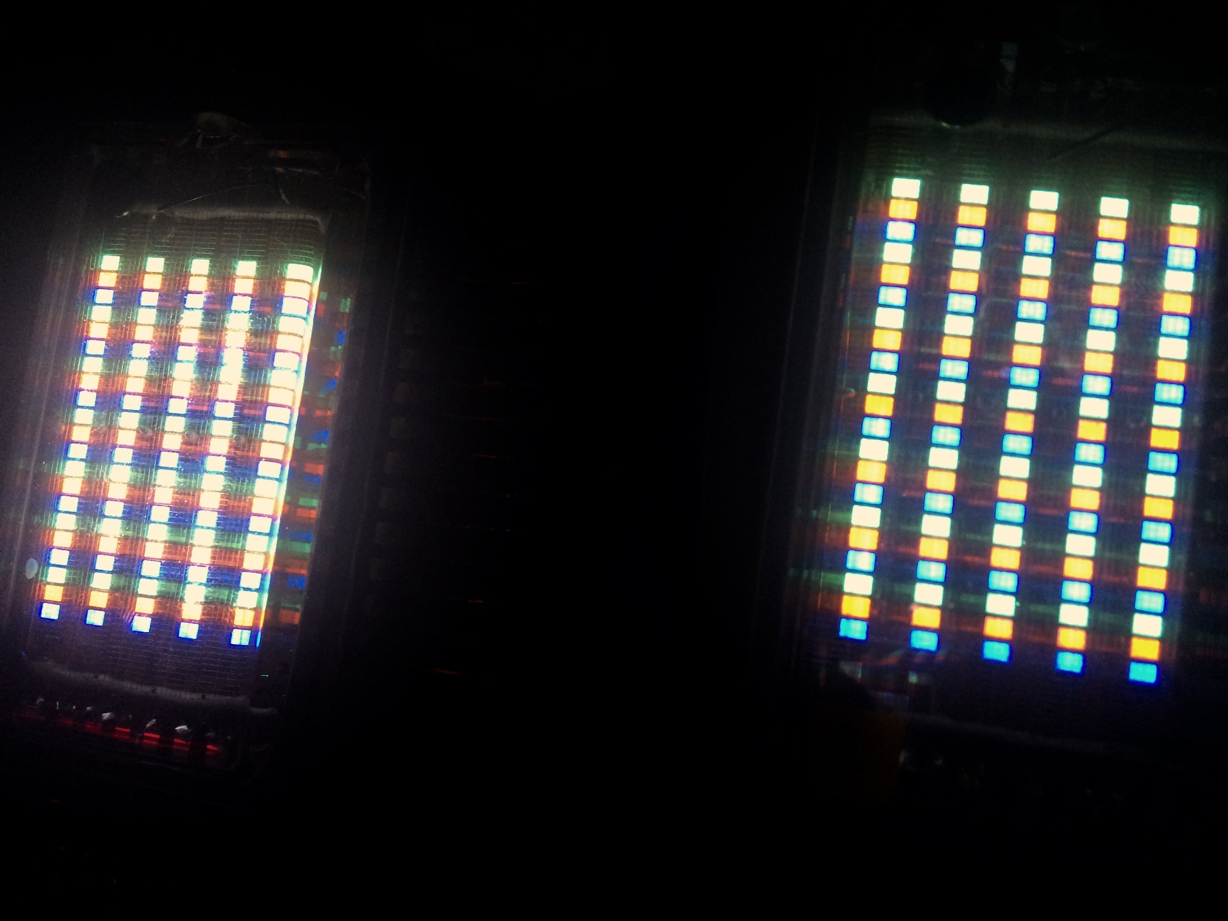
This display has 3 colors: Blue, Red, and Green. There are 5 lines with 7 of each color in each line - therefore, I have 35 Blue segments, 35 Red segments, and 35 Green segments.
This makes 105 individual segments.
There are 5 Grids, representing one (in the image below) horizontal row.
The 21 addressable pins are for the vertical rows (called "lines" in the datasheet), 1 pin per color, per row.
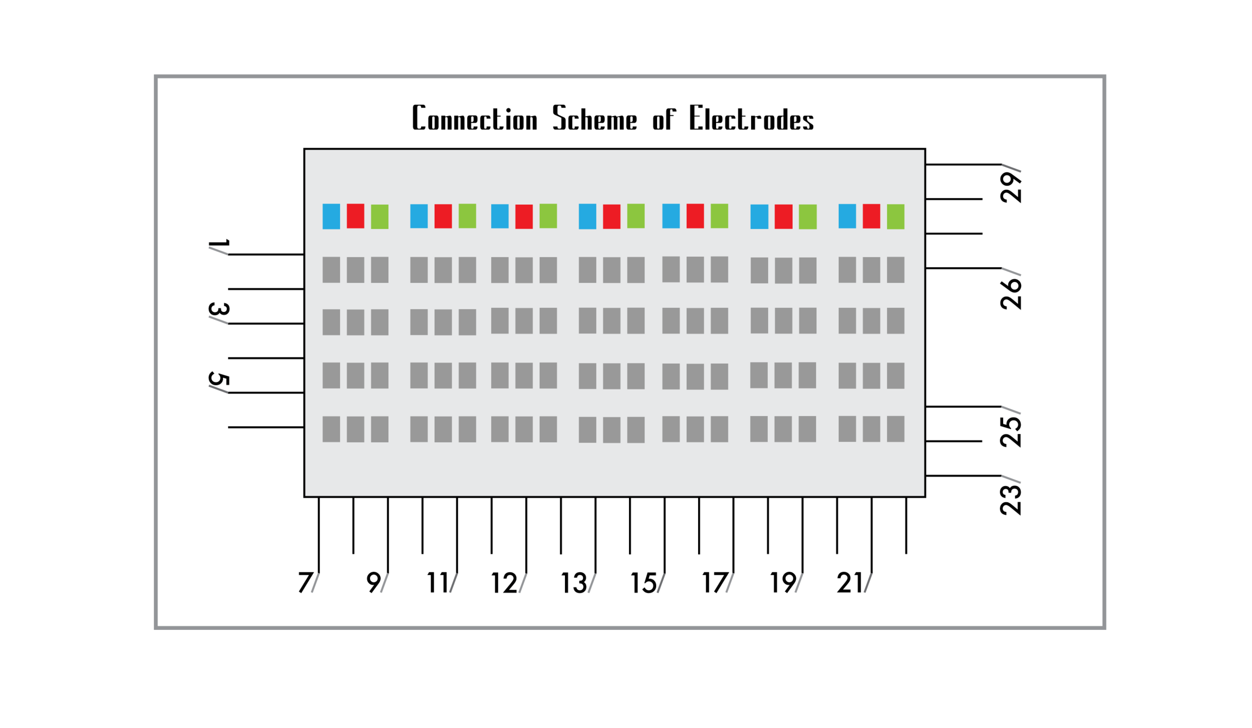
By turning on the blue line 1 and grid row 1, I can individually turn on the top left most blue segment. I will want to use other lines and grids - I will send a binary code through a micro-controller [0, 0, 0, 0, 1]. This would bypass the first 4 blue segments (those on the left most side of the VFD) and only light the last blue segment - while enabling other grid (row) activity on the first vertical line.
The Datasheet Provides Electrical Parameters as Follows:
Current Glow: 225mA Voltage Glow: 2.8v (filament specs)
Impulse current of elements of no more than mA
green glow: 7mA
red glow: 10mA
blue glow: 10mA
Impulse (pulsed) elements of voltage - the voltage of the elements pulsed
green glow: 25v
red, blue glow: 50v
Impulse GRID current of no more than: 10mA
Impulse GRID voltage: 25v

The enclosure is designed so that the leads from the VFDs are opposite and their orientations in Z are transposed. The below image is the wiring diagram for the enclosure

Beginning the wiring and coding. I tested the transistor circuitry to control the grids with some LEDs.
TRANSISTORS:
The Russian VFD has five lines of segments of colors. By switching the grids on and off I can multiplex the component.
Each Grid gets a circuit which is comprised of one TIP120 - (NPN), two 10K resistors, and an IRF9510 - (Here is a nice write up of a Mosfet PNPs and a nice Youtube Video by L. Loflin using more succinct language and maths for PNP Transistors in general).
The below graphic is the circuit driving each element (grid, green, red, and blue).
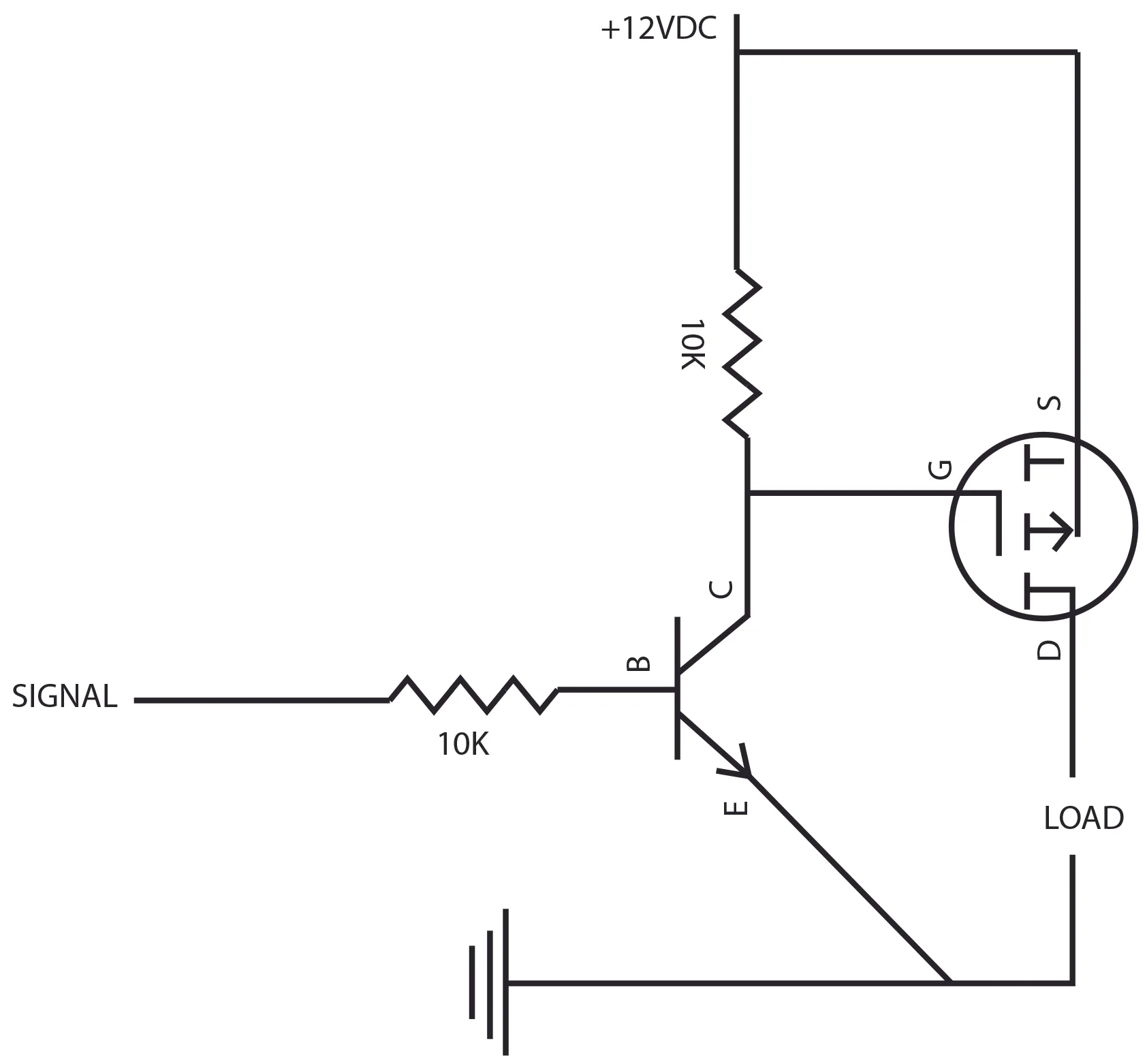
Because of size constraints for the enclosure, I purchased some SMD IRF9510s in the form of D2Paks.(this footprint is HUGE)
The TIP120 is now an outdated, no longer manufactured component (to my knowledge). There are no SMD versions of TIP120s. I purchased several N-type BJTs which have similar electrical attributes. The FZT851CT-ND worked just fine.
I air wired these and tested output coming from the teensy - to confirm the current from the Teensy would trigger this NPN.

—=-

The PNP SMD ICs I had spec’d for this project are power transistors and are built to manage high loads. This Circuit is not at all in any need of a transistor with such a large window of operational amperage. They have a large footprint because of their capacity and have a corollary cost. As such, I found a smaller form factor PNP for a 1/3 of the cost per IC - Diodes Incorporated: BSS84.

one PNP/NPN switch config
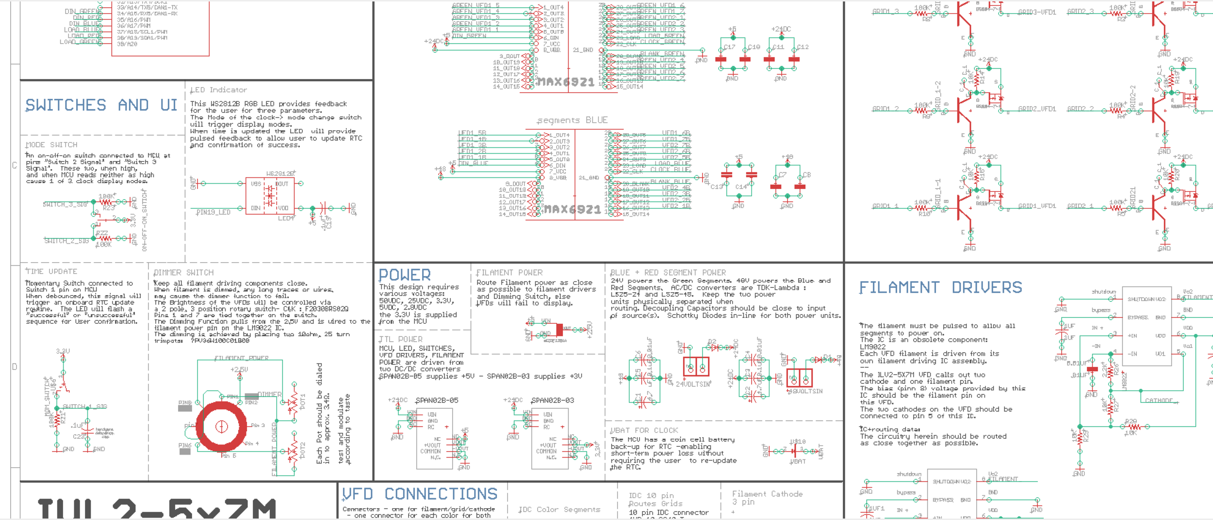
MAX6921:
I am using a MAX6921 20 output VFD driver chip.
Two MAX6921 ICs will handle the Blue and Red Segments (both driven with 50 volts at 10mA). There are seven of each, totaling 14 Outs from the 6921 IC. To drive two VFDs I double this number and have a total of 28 segments to drive, requiring 2 MAX6921 chips.
The Green Segments accept 25 volts and cannot be driven by the same MAX6921 chip driving the other segments and thus need to be driven from a separate IC with its own VBB. I will have 14 total green segments to drive (driving 2 VFDs per clock).
I have decided, for ease of coding coupled with the electrical parameters requiring the Green Segments to be driven by a separate chip, to segregate these three MAX6921 ICs to handle colors only. (one MAX6921 for Blue, one for Red, and one for Green)
The Grids (5 rows, 5 Grids) will be directly driven from the Teensy 3.6, using the NPN / PNP graphic above.
I could have coupled the Grids to be driven to the green segment 6921 IC, but for a myriad of reasons, I have chosen to keep the grids independent of the segments.
EACH MAX6921 CHIP HAS DATAIN, CLOCK, LOAD, DATAOUT, AND BLANK -
The DataIn pin, accepts the bits (send the array)
The Clock pin clocks these bits to the chip on the rising edge (meaning, every time you want to display the bit, you have to turn the clock HIGH - and then LOW as before you want to move onto the next bit to display)
- i.e. - DATAIN -> 1bit -> CLOCK HIGH -> CLOCK LOW
The Load pin pushes the bits to the segment (i.e. turns the display on) when HIGH. Make the Load pin LOW before reading new data (like a bang).
-i.e.- cycled through all bits in the above step and then -LOAD HIGH -LOAD LOW
The Blank pin resets the Clock and Load when HIGH.
Initial Power-Up and Operation
An internal reset circuit clears the internal registers of the MAX6921 - on power up. All outputs OUT0 to OUT19 and the interface output DOUT (MAX6921 only) initialize low regardless of the initial logic levels of the CLK, DIN, BLANK, and LOAD inputs.
FILAMENT:
The Filament is likely the most difficult item to drive. It is finicky - and should be considered when driving VFDs.
Driving the filament improperly will case permanent damage to the device (if not egregious, it will occur over a longer period of time).
The filament should be thought of as an Incandescent light bulb, it is only a bit of tungsten, and can consume ample amounts of current. As the wire heats, it can consume more etc. Therefore it is imperative to restrict the current going to the filament.
The Noritake site describes the ideal characteristics required to drive a filament and mentions the ideal frequency to drive the filament and that the filament should be driven with a biased DC source.
The filament on this VFD MUST be pulsed to allow all segments to power on. When driving the Filament from straight DC, the VFD will behave inaccurately. Pulsing is required to run this component long term, but if you are working with a VFD and attempting to prototype whilst Direct Current driving filament, and you can't seem to make the display function, this may be why.
The ILV2-5x7M provide data about only ONE of the pins are designated a filament pin. After reviewing the datasheet, the bias voltage provided by this IC should be used for the filament. A simple conductivity test confirmed that the two “cathodes” on the VFD itself are connected to the filament. The VFD google-translated datasheet refers to the filament as: “cathode of the extension of the inner surface of the cylinder.”
—LM9022 IC_ FILAMENT DRIVER
In some investigations of best circuitry to apply for this AC filament drive, I stumbled across this amazing blog: KevinRye.net

Kevin Rye’s Filament Driver Circuit
He implements a LM9022 VFD Filament Driver IC into his project. These ICs are obsolete, but a quick Ebay search led me straight to many options for new-old-stock. With some simple discreet components I should be oscillating awesomely for my circuit.

The circuit above calls for two filament pins. I have two cathode pins. Connecting Pin 8 of the LM9022 to what I have been calling a filament and connecting the two cathode pins to pin 5.

The cathode and the “filament” are transposing their polarity. They are phase locked outputs offset from one another - generating a sine which allows the tungsten to pulse with gradual on/off states.
DIMMER WITH Filament
The Filament power is coming from a the Monolithic Power Systems : MEZD71201A-E voltage converter - by putting resistors on the output voltage feeding the filaments I can easily and reliably control how bright these displays are.
I am using a 3 position rotary knob (C&K : F20308RS02Q) to allow the user to switch from ON / DIM / DIMMEST.
I chose to dim the filament. This may be a silly choice, but I feel it is the most isolated in its function and is already isolated in the design above that this choice made sense.
However, the wattage going to the filament is very small. The current resistors I tested would need to be extremely well toleranced with ranges of .5Ω to 1.5Ω.
These don’t exist - so I spec’d a trimpot - 25 turn, 10Ω. — > Bourns PV36W100C01B00

The design has a filament driver on both sides of the PCB. However, when dimming the filament, the power to the filament is on the right-most side of the PCB - the build up of resistance for the Filament on the left side of the PCB is unable to reach the IC. (i.e. when the dimmer switch is anything less than 100% bright, only the VFD driven by the IC close to the 2.5VDC voltage source lights).
Real time CLOCK - TEENSY 3.6 ONBOARD:

The Teensy 3.6 has a built in RTC. The library which utilizes the time function within the RTC is the Time library.To retain the Time set when configured, the Coin Cell Battery can power the RTC without powering the entire Teensy.
POWER CONSIDERATIONS:
The VFDs and the Circuit I’ve designed require various voltages:
50VDC, 25VDC, 3.3VDC, 5VDC, 2.8VDC
I have found some small form-factor 48 VDC power supply (TDK-Lambda : LS25-48) and in the same form-factor a 24 VDC power supply (TDK-Lambda : LS25-24). The 5VDC are my favorite little bricks: Mean Well’s SPAN02B-05. The 3.3v are only for MCU signal and an LED, this will be driven from the Teensy 3.6. For the Filament power I opted to drive it not from a voltage divided/ current resistors but from a Monolithic Power Systems : MEZD71201A-E.
DECOUPLING CAPACITORS:

SCHOTTKY DIODES on 48/24VIN

PROGRAMMING AND TEENSY POWER:
Note: Teensy 3.6 is not 5V tolerant.

To ensure users of the clock do not accidentally program the Teensy while still powered- causing a surge of energy, cut the trace referenced in the below image.
MODE SWITCHES / UPDATE TIME Switches


WS2812B

https://github.com/SamEA/WS2812 - using WS2812B for indication of mode and to indicate when time is being updated —> programmable RGB - link provides schema and eagle lib for LED.
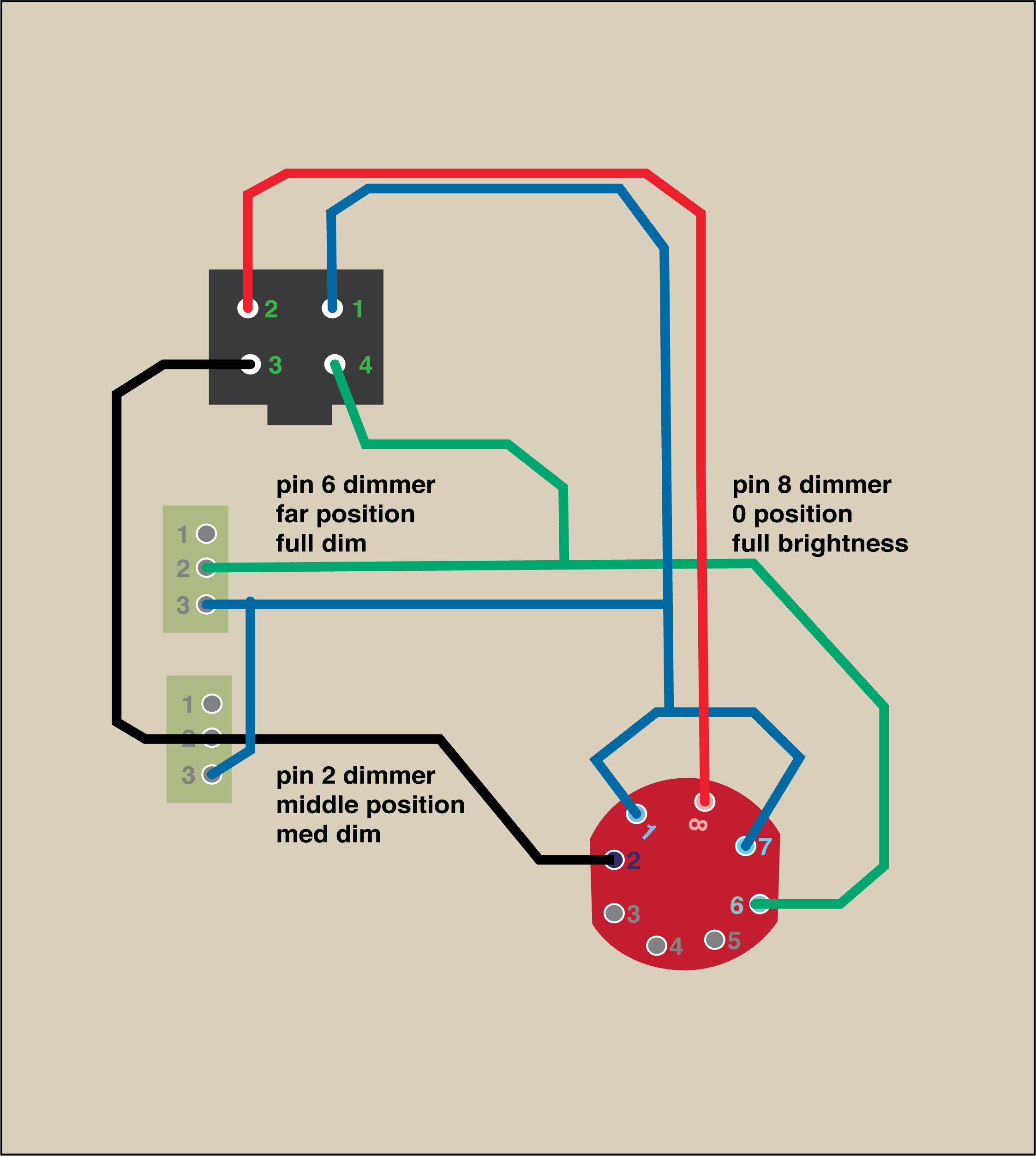
connectors + hardware:

The wiring lends itself to IDC connectors. The orientation of the VFDs in the housing I’ve designed has the 2nd one flipped 180°. The MAX6921 IC’s are designated per color. The grids are driven from NPN/PNP signals.
To keep it straight, I have organized the wiring pin-outs to be organized accordingly.
The colors for both VFDs are organized with one IDC and are in order of orientation in the display.
The grids are also organized in order of display.
Full Schematic PDF found HERE

—ENCLOSURE—


Links for Casting with Silicone and Resin:
Guerrilla Guide - Excellent glossary of terms
Pressure Pot/Vacuum Chamber - Clear explanation of tools / when/why to use them.

Test fit (above) from FormLabs Form2 Resin Printer- snaps together well. A touch of material removal here and there - but good fit.
-
*I ended up reprinting edited versions of these to account for slight design changes and for a few essential DFM modifications. As such positives may have various versions etc.
<< Positive Prep for Casting >>
As I am using crystal clear resin, I want to ensure that the mold has the best possible version of the objects — no pit marks, filled, wet sanded, and buffed. -that water look-

It is ever so difficult to sand and buff (subtractive) to attain smooth crystal clear surface finish.
Additive to fill gaps - even those unseen- is a requirement.
It is to fill the sanded elements with a high build primer which has enough body and self levels which makes a wonderfully matte but even and lovely finish.
—

SEM High-Build Primer/Surfacer is a touch expensive for primer, but well well worth the couple extra bucks. It adheres well, sands super awesome and is a perfect product for models of this size.
Then for the gloss effect:
Spraymax 3680061 2K Clear Glamour high gloss paint - is badass - but adds substantial thickness to the parts, as such I decided I cannot afford to loose those tolerances to an aesthetic so I ended up looking for alternatives.
Caranuba Wax rubbed into the flat/matte sanded positives provides me with a fairly awesome finish.
—
IMPORTANT!
Be sure to do a cure inhibition test for all chemicals applied to ensure silicone and resin are not inhibited from chemicals contained within any processing done.
There are many known chemicals to cause inhibition in addition curing silicones. Addition cure silicones use a platinum catalyst which reacts to effect the curing reaction when the “A” component is mixed with the “B” component. The platinum can become deactivated by coming in contact with certain chemical species. Once the catalyst is deactivated or poisoned, the affected area of silicone may never cure to the proper state of cure – meaning the inhibited area may stay runny, sticky, or fluid.
3D PRINTED COMPONENT TEST FIT and ACCURATE HOLE MAKING:


I made a jig to hold the components straight for drilling the holes which mate the front and back sections of the enclosure (above).
For accurate holes, both for dimensionality and symmetry, should be made with drills or machined.
—
I fit test the back components (AC cable gland, AC switch, reprogram momentary switch, Battery, and USB).
<< Casting SILICONE/MOTHER >>
I will be casting several silicone molds for the resin parts.
Considerations for materials used (both what resin and subsequently choosing accurate silicones) must be made from the start. As the components and the properties of the resin are likely far more important than constraining the resin to a specific silicone.
I identified a specific resin for several reasons - these are common considerations for you to select the resin you wish to use. - UV Resistance - Shrinkage - Shore Hardness - (and other mechanical properties such as flex and strength under flex).
In tandem, considering minimum and maximum thicknesses for the resin must be confirmed before selection.
I am not a fan of the super-bad-for-you elements of the majority of crystal clear casting resins. As such I plan to use Entropy Resins - Super Sap CCR - a Bio Based crystal clear casting resin with much less health risk and better for our planet. (Datasheet)
This resin calls for the use of a Platinum Cure Silicone. Because of the tight tolerances of the enclosure, I can tolerate very little shrinkage. I found the PlatSil product line and based on the hardness of the silicones have chosen three types.PlatSil 73-25 / PlatSil 73-45 / PlatSil 73-15
These videos are BY FAR the best tutorials for how to glean the logic of casting.
Mother Molds for tight tolerance fits must keep the silicone mold from warping when positive is removed, and must retain registration when silicone is removed from mother mold.
I kept trying, for this finicky component, to use FDM prints in conjunction with laser cut or CNC routed parts as a mother. However, the specificity of the holes and inserts mean the slop and inherent nature of FDM printing kept me from having repeatable and reliable enough casting processes.

So -> worn out from the four hardcore attempts to do what I needed and get the results from the above attempts - I decided to create a better mouse trap.
Knowing that SLS printing is far more robust in both tolerances and in structural integrity, I designed the below assembly to ensure I was able to use precision and threaded features into the enclosure itself vs. epoxying plastic inserts into semi-stable PLA with super loose tolerances and unaccepting of robust manipulation.


I incorporated many redundant constraints which acommodate accurate fitting when disassembly/reassembly for the many pulls I plan on making.
ONE: I was able to tap the mother and not rely on threaded inserts. this provided me with reliable hole positioning and clamping in accurate placement.
TWO: incorporation of dowels to register the assembly before using screws to secure the assembly. This gives me strain relief on the threads and provides additional registration.
THREE: upgrading inserts for holes in component which provides accurate placement of the holes and proper depth position for non-thru hole features.
FOUR: draft angles incorporated for seating assembly of mother mold and confirming proper reassembly.

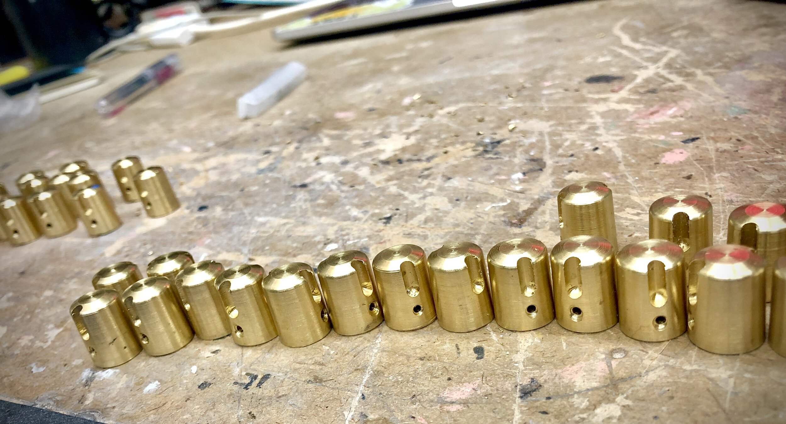
Brass Knob Machining for dimmer switch && brass Feet for enclosure:


___